Project Overview
The goal of this project was to create a circuit that would display your date of birth on a seven segment display controlled by three switches. We first had to create a truth table, then come up with the minterms for the circuit using k-mapping. Then we took these minterms and tested the circuit in Multisim, then once it worked in multisim we bread-boarded the circut.
Problem Conception via Truth Table
In this project I used a truth table to allow me to figure out which segments (A-G) on the seven segment needed to be lighted in order to display each digit in my birth date.

The columns X Y Z represent each of the switches and the columns A-G represent the segments in the seven segment display. The 1's and 0's under the X Y Z column mean a switch is on or off and the 1's and 0's under A-G mean that a segment is lit or unlit. The x's at the bottom represent digits that do not matter, and will not be included in the minterms because they are not relevant to the output.
Karnaugh Maps and Simplified Logic

|
K-mapping takes a truth table and puts it in a format where the 1 outputs are able to be grouped to create minterms. Each column from each A-G term is translated into a 2x4 K-map with XY terms ion the vertical side and Z on the horizontal.
Since there are 8 digits for each segment, the first tow go in the top row, the second two go in the third row, the third two go in the bottom row, and the fourth two go in the third row. Then group the largest possible groups of 1's in order to get all ones included in the minterm. (x's can be treated as 1's if it allows a larger blocking to be created, however it is no necessary that all x's are grouped. ) Each K-map gives an equation for a segment which can then be translated into a circuit in multisim. |
Multisim Circuit
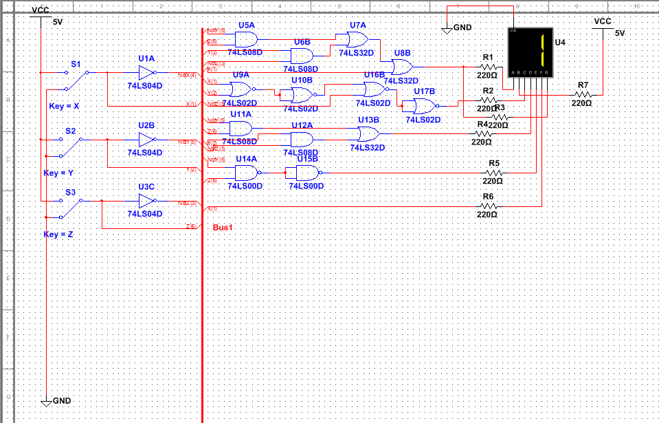
Next, I created a circuit in Multisim. I put my circuit in bus form so that it was easier to keep the wires separated. The circut required 4 2-input and gates, 3 2-input OR gates, 4 2-input NOR gates and 2-input NAND gates. This means I would need 1 NAND, NOR, AND, NOR, and INV gate each. Both the NAND and NOR circuits were longer because of this, but none of my AOI circuits could be simplified by NAND or NOR. I used a common cathode display, which because it is grounded, must recieve power to display light.
Bill of Materials
DOB Bill of Materials
74LS04 IC
74LS00 IC
74LS02 IC
74LS08 IC
74LS32 IC
PLD (breadboard)
Wires (around 100)
Power Source
74LS04 IC
74LS00 IC
74LS02 IC
74LS08 IC
74LS32 IC
PLD (breadboard)
Wires (around 100)
Power Source
Breadboarding
When breadboarding, the first step I took was placing the IC chips so that I could wire the equations for each segment of the seven seg display. Then I separately grounded and powered each chip and connected the entire board to a power and ground. I had to go back and rewire the entire board again because I had made a mistake on segment C that I didn't originally find.
Conclusion
This project was probably the most difficult that we have done so far. I had to do the most troubleshooting on this project. I tried building the circuit in Multisim without a bus which quickly became confusing so I had to go back and do the equations with a bus. Then, because the breadboard had so many wires and so many chips, I didn't get the entire seven seg to work right until the third time I rewired it. One of the biggest things I learned with this project is to make sure that you are making your circuits as simple as possible in order to reduce the amount of mistakes you could make. If i had to do this project again, when I was breadboarding I would color code the breadboard wires by segment so that I could better check it if I made a mistake. I don't really have any questions about the project besides whether it may be helpful to space out the IC chips to make it more neat.
